Tags Posts tagged with "Kevin Yager"

Kevin Yager

Members of the quantum materials team, from left, Gregory Doerk, Jerzy Sadowski, Kevin Yager, Young Jae Shin and Aaron Stein. Photo from BNL

By Daniel Dunaief

Henry Ford revolutionized the way people manufactured cars through automation, speeding up the process, reducing waste and cutting costs.

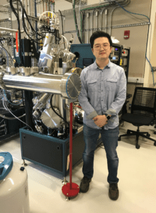
Similarly, at Brookhaven National Laboratory, researchers like the newly hired Young Jae Shin, who is a staff scientist at the Center for Functional Nanomaterials, hopes to improve the process of automating the handling of thin flakes of material used in a next generation technology called quantum information science, or QIS.

Working with scientists at Harvard University and the Massachusetts Institute of Technology, Shin is looking for ways to handle these flakes, which are one atom thick, of two-dimensional layers from different materials. Stacked together, these flakes can help create structures with specific electronic, magnetic or optical properties that can be used as sensors, in communication, or encryption.

Young Jae Shin at Harvard University, where he was a post doctoral researcher. Photo from Y. Shin

“Researchers are building these kinds of customized structures manually now,” explained Kevin Yager, leader of the CFN Electronic Nanomaterials Group, in an email. “QPress [Quantum Material Press] will allow us to automate this.” At this point, QPress is just starting, but, if it works, it will “absolutely allow us to accelerate the study of these materials, allowing researchers to find optimal materials quickly,” Yager continued.

Theoretically, quantum computers overcome the limitations of other systems, Shin explained.

The flakes come from the exfoliation of thin structures taken from a bulk material. This is akin to a collection of leaves that fall around trees. According to Yager, the structures scientists hope to make would be akin to a collection of leaves from different trees, put together to make a new structure or material with specific properties. “The idea is for the robot to sift through the flakes, and identify the ‘best’ ones and to stack these together into the right structure. The ‘stacking’ will involve combining flakes of different materials,” he said.

The less desirable flakes typically are the wrong size, have tears, ripples or other defects and have contaminants. Groups of scientists are predicting the kinds of layered designs that will have desired properties.

Shin suggested that the CFN supports the needs of the end user community, as CFN is a “user-based facility.”

Physicists at Harvard and MIT plan to use the QPress to study unusual forms of superconductivity. By tapping into materials that conduct electricity without losing energy at lower temperatures, researchers may make progress in quantum computing, which could exceed the ability of the current state-of-the-art supercomputers.

Stacking the flakes can create new materials whose properties not only depend on the individual layers, but also on the angle between the stacks. Scientists can change one of these new structures from having metallic to having insulating properties, just by altering the relative angle of the atoms. The challenge, however, is that putting these fine layers together by hand takes time and generates errors which, BNL hopes, an automated approach can help reduce.

“Ultimately, we would like to develop a robot that delivers a stacked structure based on the 2-D flake sequences and crystal orientations that scientists select through a web interface” to a machine, Charles Black, the head of the Center for Functional Nanomaterials at BNL, explained in a recent BNL feature. “If successful, the QPress would enable scientists to spend their time and energy studying materials, rather than making them.”

Barring unforeseen delays, scientists anticipate that they will be able to build a machine that creates these flakes, catalogs them, stacks them and characterizes their properties within three years. These functions will be available online in stages, to allow the use of the QPress prior to its completion.

Each stage in the QPress process uses computer software to reduce the effort involved in generating and interpreting usable structures.

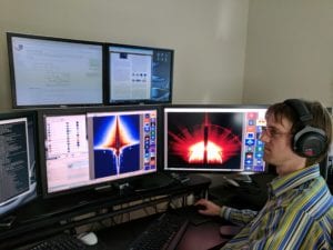
Minh Hoai Nguyen, an assistant professor in the Department of Computer Science at Stony Brook University and doctoral student Boyu Wang from the Computer Vision Lab at SBU are creating a flake cataloger, which will use image analysis software to scan and record the location of flakes and their properties.

“The flakes that scientists are interested in are thin and thus faint, so manual and visual inspection is a laborious and error-prone process,” Nguyen said in the BNL feature.

At BNL, Shin is one of three scientists the Upton-based facility is hiring as a part of this effort. They are also seeking robot or imaging process experts. Shin has “been in the CFN just a short while, but is already having an impact- — for instance, allowing us to handle classes of two-dimensional materials that we were not working with before,” Yager said.

The field of quantum information science is extremely competitive, with researchers from all over the world seeking ways to benefit from the properties of materials on such a small scale. The United States has been investing in this field to develop leadership science in this area.

The University of Tokyo has developed an automation system, but Shin explained that it is still not perfect.

Yager said that numerous unknown applications are “waiting to be discovered. Researchers are working hard on real quantum computers. Prototypes already exist but creating viable large-scale quantum computers is a major challenge.”

A resident of on-site housing at BNL, Shin was born in the United States and grew up in Korea. He is married to Hyo Jung Kim, who is studying violin at Boston University. 

As for the work Shin and others are doing, Yager suggested that the effort has generated considerable interest at the CFN.

“There is huge excitement at BNL about quantum research broadly and QPress in particular,” said Yager. Shin is “a big part of this — bringing new technical knowledge and new enthusiasm to this ambitious project.”

From left, BNL Staff Scientist Lihua Zhang, former postdoctoral researcher Vitor Manfrinato and BNL Senior Scientist Aaron Stein. Photo courtesy of BNL

By Daniel Dunaief

It took a village to build this particular village or, more precisely, a pattern so small it could fit thousands of times over on the head of a pin.

Working at Brookhaven National Laboratory’s Center for Functional Nanomaterials, a team of researchers wanted to exceed the boundaries of creating small patterns with finely honed features. The group included Aaron Stein, a senior scientist at CFN, Charles Black, the head of CFN, Vitor Manfrinato, a former postdoctoral researcher at BNL and several other key members of the BNL team. The team added a pattern generator that allowed them to control a microscope to create a pattern that set a record for drawing at the 1-nanometer scale.

Just for reference, the width of a human hair is about 80,000 to 100,000 nanometers. The size of the pattern is a breakthrough as standard tools and processes generally produce patterns on a scale of 10 nanometers. “We were able to push that by a factor of five or 10 below,” Stein said. “When you get to those small size scales, that’s pretty significant.”

In this case, the novelty that enabled this resolution originated with the idea of employing the scanning transmission electron microscope, which isn’t typically used for patterning to create these images. The scanning transmission electron microscope has an extraordinarily high resolution, while the pattern generator allowed them to control the patterns they drew and other aspects of the exposure.

Researchers at CFN are focusing on this spectacularly small world to manipulate properties such as chemical reactivity, electrical conductivity and light interactions. “This new development is exciting because it will allow other researchers to create nanomaterials at previously impossible size scales,” Kevin Yager, a group leader at CFN explained in an email. “There are numerous predictions about how materials should behave differently at a size scale at 1 to 3 nanometers. With this patterning capability, we can finally test some of those hypotheses,” he said.

Stein and the research team were able to create this pattern on a simple polymer, polymethyl methacrylate, or PMMA for short. “It’s surprising to us that you don’t need fancy materials to create these kinds of features,” said Stein. “PMMA is a common polymer. It’s Plexiglas. It’s kind of exciting to do something that is beyond what people have done” up until now.

One of the many possible next steps, now that the researchers have developed this proof of principle, is to apply this technique to a substance that might have commercial use. Taking the same approach with silicon, for example, could lead to innovations in electronics. “We can make them with a high clarity of patterns and sharp corners, which we can’t do with other techniques,” Stein said.

The BNL research team would “like to apply this to real world research,” which could include electronics and transistors, as well as photonics and plasmonics, he added. This project arose out of a doctoral thesis that Manfrinato was conducting. He is one of the many scientists who came to BNL, which isa Department of Energy funded user facility that provides tools to conduct research for scientists from around the world.

Manfrinato was a doctoral student in Professor Karl Berggren’s group at the Massachusetts Institute of Technology. In an email, Manfrinato explained that he was interested in pushing the resolution limits of e-beam lithography. “BNL has state of the art facilities and expert staff, so our collaboration was a great fit, starting in 2011,” he explained.

Other scientists thought it was worthwhile to continue to pursue this effort, encouraging him to “come here and work on this. It’s a home grown project,” Stein said. Manfrinato worked on his doctorate from 2011 to 2015, at which point he became a postdoctoral researcher at BNL. His efforts involved several groups, all within the Center for Functional Nanomaterials at BNL. Stein, Manfrinato and Black worked on the lithography part of the project, while Lihua Zhang and Eric Stach developed the microscopy. Yager helped the team to understand the processes by which they could pattern PMMA at such small scale lengths.

“No one or two of us could have made this happen,” Stein said. “That’s really the joy of working in a place like this: There are [so many] permutations for collaborating.” Indeed, the other scientists involved in this study were Yager; Zhang, a staff scientist in electron microscopy; Stach, the electron microscopy group leader at CFN; and Chang-Yong Nam, who assisted with the pattern transfer.

Manfrinato, who is now a research and development engineer at a startup company in the San Francisco Bay area, explained that this lithographic technique has numerous possible applications. Other researchers could create prototypes of their devices at a level below the 10-nanometer scale at CFN. Manfrinato interacts with the BNL team a few times a month and he has “exciting results to be further analyzed, explored and published,” he wrote in an email.

Stein said BNL would like to offer this patterning device for other users who come to BNL. Ultimately, researchers use materials at this scale to find properties that may vary when the materials are larger. Sometimes, the properties such as color, chemical reactivity, electrical conductivity and light interactions change enough to create opportunities for new products, innovations or more efficient designs.

A resident of Huntington, Stein and his wife Sasha Abraham, who works in the planning department for the Town of Huntington, have a 15-year-old daughter Lily and a 13-year-old son Henry.

As for his work, Stein said he’s interested in continuing to push the limits of understanding various properties of nanomaterials. “My career has been using the e-beam lithography to make all sorts of structures,” he said. “We’re in a regime where people have not been there before. Finding the bottom is very interesting. Figuring out the limits of this technique is, in and of itself” an incredible opportunity.

Standing near one of the X-ray scattering instruments, Kevin Yager holds a collection of samples, including a self-assembling polymer film. Photo courtesy of BNL

By Daniel Dunaief

Throw a batch of LEGOs in a closed container and shake it up. When the lid is opened, the LEGOs will likely be spread out randomly across the container, with pieces facing different directions. Chances are few, if any, of the pieces will stick together. Attaching strong magnets to those pieces could change the result, with some of the LEGOs binding together. On a much smaller scale and with pieces made from other parts, this is what researchers who study the world of self-assembled materials do.

Scientists at the Center for Functional Nanomaterials and at the National Synchrotron Light Source II at Brookhaven National Laboratory experiment with small parts that will come together in particular ways based on their energy landscapes through a process called self-assembly.

Every so often, however, a combination of steps will alter the pathway through the energy landscape, causing molecules to end up in a different final configuration. For many scientists, these so-called nonequilibrium states are a nuisance.

Above, Kevin Yager listens to sonified data. When data is sonified, it is translated into sound. Photo by Margaret Schedel

For Kevin Yager, they are an opportunity. A group leader at the CFN who works closely with the NSLS-II, the McGill University-educated Yager wants to understand how the order of these steps can change the final self-assembled product. “In the energy landscape, you have these peaks and valleys and you can take advantage of that to move into a particular state you want,” Yager said. “The high level goal is that, if we understand the fundamentals well enough, we can have a set of design rules for any structure we can dream up.”

At the CFN, Yager manages a nanofabrication facility that uses electron-beam lithography and other techniques to make nanostructures. He would like to fabricate model batteries to show the power of nanomaterials. He is also determined to understand the rules of the road in the self-assembly process, creating the equivalent of an instruction manual for miniature parts.

In future years, this awareness of nonequilibrium self-assembly may lead to revolutionary innovations, enabling the manufacture of parts for electronics, drugs to treat disease and deliver medicine to specific locations in a cell and monitors for the detection of traces of radioactivity or toxins in the environment, among many other possibilities.

Yager’s colleagues saw considerable opportunities for advancement from his work. Nonequilibrium self-assembly has “significant potential for a broad range of nanodevices and materials due to its ability to create complex structures with ease,” Oleg Gang, a group leader in Soft and Bio Nanomaterials at the CFN, explained in an email. Yager is an “excellent scientist” who produces “outstanding results.”

One of the things Yager hopes his research can develop is a way to “trick self-assembly into making structures they don’t natively want to make” by using the order of steps to control the final result.

As an example, Yager said he developed a sequence of steps in which nanoscale cylinders pack hexagonal lattices into a plane. These lattices tend to point in random directions as the cylinders form. By following several steps, including sheer aligning a plane and then thermal processing, the cylinders flip from horizontal to vertical as they inherit the alignment of the sheered surface. Flipping these cylinders, in turn, causes the hexagons all to point in the same direction. When Yager conducted these steps in a different order, he produced a different structure.

Broadly speaking, Yager is working on stacking self-assembling layers. In his case, however, the layers aren’t like turkey and swiss cheese on a sandwich, in which the order is irrelevant to the desired final product. Each layer has a hand in directing the way the subsequent layers stack themselves. Choosing the sequence in which he stacks the materials controls their structure.

Yager is working with Esther Takeuchi and Amy Marschilok at Stony Brook University to develop an understanding of the nanostructure of batteries. Gang suggested that Yager’s expertise is “invaluable for many scientists who are coming to the CFN to characterize nanomaterials using synchtrotron methods. In many cases, it would probably be impossible to achieve such quantitative understanding without [Yager’s] input.”

Yager and his wife Margaret Schedel, an associate professor in the Department of Music at Stony Brook University who is a cellist and a composer, live in East Setauket. The couple combined their talents when they sought ways to turn the data produced by the CFN, the NSLS and the NSLS-II into sound.

Scientists typically convert their information into visual images, but there’s “no reason we can’t do that with sound,” Yager said. “When you listen to data, you sometimes pick up features you wouldn’t have seen.”

One of the benefits of turning the data into sound is that researchers can work on something else and listen to the collection of data in the background, he said. If anything unexpected happens, or there is a problem with a sample or piece of equipment, they might hear it and take measures more rapidly to correct the process. “This started as a fun collaboration,” Yager said, “but it is useful.”

Schedel is working on sonifying penguin data as well. She also sonified wave data on Long Island. “By listening to the tides quickly, larger patterns emerge,” she said, adding that Yager thought the idea was theoretically interesting until he listened to misaligned data and then he recognized its benefit.

Schedel’s goal is to see this sonification effort spread from one beamline to all of them and then to the Fermilab near Chicago and elsewhere. She wants sonification to become “an ear worm in the science community.”

While Schedel introduced Yager to the world of sound in his research, he introduced her to sailing, an activity he enjoyed while growing up in the suburbs of Montreal. When she sails with him, they are “half in and half out of the boat,” Schedel said. It’s like two people “flying a kite, but you are the kite. You have to learn how to counterbalance” the boat. They hike out so they can take turns faster without tipping over, she said.