By Daniel Dunaief
It took a village to build this particular village or, more precisely, a pattern so small it could fit thousands of times over on the head of a pin.
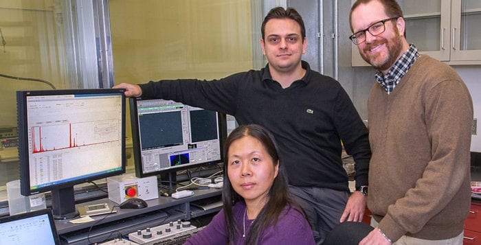
Working at Brookhaven National Laboratory’s Center for Functional Nanomaterials, a team of researchers wanted to exceed the boundaries of creating small patterns with finely honed features. The group included Aaron Stein, a senior scientist at CFN, Charles Black, the head of CFN, Vitor Manfrinato, a former postdoctoral researcher at BNL and several other key members of the BNL team. The team added a pattern generator that allowed them to control a microscope to create a pattern that set a record for drawing at the 1-nanometer scale.
Just for reference, the width of a human hair is about 80,000 to 100,000 nanometers. The size of the pattern is a breakthrough as standard tools and processes generally produce patterns on a scale of 10 nanometers. “We were able to push that by a factor of five or 10 below,” Stein said. “When you get to those small size scales, that’s pretty significant.”
In this case, the novelty that enabled this resolution originated with the idea of employing the scanning transmission electron microscope, which isn’t typically used for patterning to create these images. The scanning transmission electron microscope has an extraordinarily high resolution, while the pattern generator allowed them to control the patterns they drew and other aspects of the exposure.
Researchers at CFN are focusing on this spectacularly small world to manipulate properties such as chemical reactivity, electrical conductivity and light interactions. “This new development is exciting because it will allow other researchers to create nanomaterials at previously impossible size scales,” Kevin Yager, a group leader at CFN explained in an email. “There are numerous predictions about how materials should behave differently at a size scale at 1 to 3 nanometers. With this patterning capability, we can finally test some of those hypotheses,” he said.
Stein and the research team were able to create this pattern on a simple polymer, polymethyl methacrylate, or PMMA for short. “It’s surprising to us that you don’t need fancy materials to create these kinds of features,” said Stein. “PMMA is a common polymer. It’s Plexiglas. It’s kind of exciting to do something that is beyond what people have done” up until now.
One of the many possible next steps, now that the researchers have developed this proof of principle, is to apply this technique to a substance that might have commercial use. Taking the same approach with silicon, for example, could lead to innovations in electronics. “We can make them with a high clarity of patterns and sharp corners, which we can’t do with other techniques,” Stein said.
The BNL research team would “like to apply this to real world research,” which could include electronics and transistors, as well as photonics and plasmonics, he added. This project arose out of a doctoral thesis that Manfrinato was conducting. He is one of the many scientists who came to BNL, which isa Department of Energy funded user facility that provides tools to conduct research for scientists from around the world.
Manfrinato was a doctoral student in Professor Karl Berggren’s group at the Massachusetts Institute of Technology. In an email, Manfrinato explained that he was interested in pushing the resolution limits of e-beam lithography. “BNL has state of the art facilities and expert staff, so our collaboration was a great fit, starting in 2011,” he explained.
Other scientists thought it was worthwhile to continue to pursue this effort, encouraging him to “come here and work on this. It’s a home grown project,” Stein said. Manfrinato worked on his doctorate from 2011 to 2015, at which point he became a postdoctoral researcher at BNL. His efforts involved several groups, all within the Center for Functional Nanomaterials at BNL. Stein, Manfrinato and Black worked on the lithography part of the project, while Lihua Zhang and Eric Stach developed the microscopy. Yager helped the team to understand the processes by which they could pattern PMMA at such small scale lengths.
“No one or two of us could have made this happen,” Stein said. “That’s really the joy of working in a place like this: There are [so many] permutations for collaborating.” Indeed, the other scientists involved in this study were Yager; Zhang, a staff scientist in electron microscopy; Stach, the electron microscopy group leader at CFN; and Chang-Yong Nam, who assisted with the pattern transfer.
Manfrinato, who is now a research and development engineer at a startup company in the San Francisco Bay area, explained that this lithographic technique has numerous possible applications. Other researchers could create prototypes of their devices at a level below the 10-nanometer scale at CFN. Manfrinato interacts with the BNL team a few times a month and he has “exciting results to be further analyzed, explored and published,” he wrote in an email.
Stein said BNL would like to offer this patterning device for other users who come to BNL. Ultimately, researchers use materials at this scale to find properties that may vary when the materials are larger. Sometimes, the properties such as color, chemical reactivity, electrical conductivity and light interactions change enough to create opportunities for new products, innovations or more efficient designs.
A resident of Huntington, Stein and his wife Sasha Abraham, who works in the planning department for the Town of Huntington, have a 15-year-old daughter Lily and a 13-year-old son Henry.
As for his work, Stein said he’s interested in continuing to push the limits of understanding various properties of nanomaterials. “My career has been using the e-beam lithography to make all sorts of structures,” he said. “We’re in a regime where people have not been there before. Finding the bottom is very interesting. Figuring out the limits of this technique is, in and of itself” an incredible opportunity.


