BNL’s Sadowski studies small-scale structures
When a successful chef mixes ingredients, he changes the proportions of nutmeg to cinnamon or of parsley to oregano. He’s much more likely to focus on how the final product affects the flavor than he is the way the ingredients mix.
That’s not the case for Jurek (pronounced Yoo rek) Sadowski. Although he’s not a chef, the staff scientist at Brookhaven National Laboratory’s Center for Functional Nanomaterials (CFN) would like to understand how some of the smallest pieces of organic metal complexes come together when they go through a process called self-assembly.
“I’m not only interested in obtaining the recipe for making these [products], but I’m also interested in understanding how and why things happen in these conditions on a more basic level,” Sadowski said.
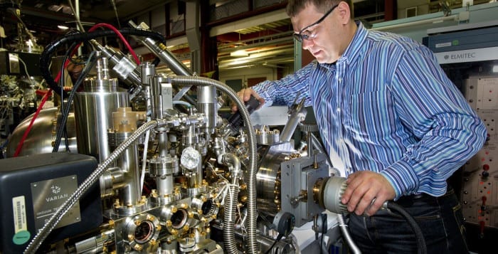
Working with the low-energy electron microscope, Sadowski is a part of a team at the CFN that is involved in seeing and interpreting changes that occur on an atomic scale.
Sadowski has collaborated on environmental products that can remove greenhouse gases like carbon dioxide from the air. This research helps understand how these self-assembled organic compounds develop pores of different sizes that can trap greenhouse gases.
The size of the pores works like a fishing net designed to catch the equivalent of Goldilocks gases from the air. Some gases pass right through them, while others bounce off without getting trapped. Then there are those, like carbon dioxide, that fit perfectly in the small spaces between the organic pieces.
In putting these products together, Sadowski asks what he needs to do to make the process more efficient and more selective.
The CFN is a user facility, which means that scientists around the world can benefit from the high level of technical expertise Sadowski possesses. He has worked with scientists from Columbia, Yale, Oak Ridge National Laboratory and SUNY facilities as well as visitors from the United Kingdom, Denmark, Germany, Italy, Croatia and Japan.

Researchers who have worked with Sadowski suggested that his scientific and technical knowledge make him a particularly effective collaborator.
The low-energy electron microscope is a “very complicated instrument,” said Richard Osgood, the Higgins professor emeritus of electrical engineering and applied physics at Columbia University, who has collaborated for years with Sadowski. “You don’t just go in and turn a dial: it’s much more complicated than that. You have to tune things up.”
Working with Sadowski greatly lowers the cost of research because he can “do something in a couple of days” that might otherwise take a graduate student or other researcher a half a year or more to figure out,” Osgood said.
Sadowski said some of the products that use self-assembly include wearable electronics, such as solar cells or clothing, or wearable medical devices.
Sadowski divides his time about equally between pursuing his own research and working with others at the CFN.
Sadowski runs his own experiments mostly in a vacuum, where he varies the temperature and the density of the molecules he’s using.
Sadowski is planning to give a talk in March at the American Physical Society meeting in Baltimore about his work.
“It’s important to understand how the molecules self-assemble themselves on the surface,” he said. “We can utilize self-assembly for further advances.”
For about five years, Sadowski has helped plan the creation of a new beamline at the National Synchrotron Light Source II at BNL. That beamline, which will be called the electron spectro-microscopy beamline, will be completed later this year. The beamline will use a microscope that the CFN is contributing, which will help provide structural, chemical and electronic maps of surfaces with a resolution of a few nanometers.
“We will have a much more extended capability for studying chemical reactions as they happen on the surface and the electronic structure of the materials” by combining information of the surface morphology with the electronic structure and chemistry. This, he said, will provide a “comprehensive picture of the surface, or of a catalyst, or of a reaction” as it’s occurring.
One of the first experiments he might do would be to provide a chemical map of the surface of a material. He plans to determine the oxidation state of metals making up the surface.
Sadowski lives on the Upper East Side of Manhattan with his wife Adrianna Sadowska (whose name is slightly different to reflect her gender). The couple met in their native Poland where he was taking a class to brush up on Japanese before moving there after he earned his Ph.D. Sadowska, who is now a wine specialist at an auction house in White Plains, was preparing for a trip to Japan as well. The two expatriates lived in Japan for almost a decade. After getting married in Japan, they came to the United States.
As for his work, Sadowski said new questions regularly inspire him. “Every day, there’s a new challenge,” he said. “I really like to solve problems, one by one.”
The work done at Sadowski’s group and at the CFN can and likely will have numerous benefits, Osgood said.
This work could “form new technology that nobody dreamed about before,” said Osgood, who was an associate director at BNL and was directly involved in the creation of the CFN. “Every time I walk out there, I kick up my heels. It’s such a wonderful facility.”


